
Tel:+86-15698999555
Email:haixin6@jzhxgs.com
Web:en.jzhxgs.cn
Ads:NO.6 ,SHENGHUA STREET,TAIHE DISTRICT, JINZHOU CITY, LIAONING PROVINCE, CHINA.
Silicon is a non-metallic element with the element symbol Si, located in the third period of the periodic table, group IVA. It has an atomic number of 14 and a relative atomic mass of 28.0855. The crystal cell is cubic diamond type. Silicon, as a dark gray crystal with a bluish luster, is the new darling of the computer age. It can be said that it injects the soul into our various electronic products.
1. Discovery
Silicon first appeared in the form of silicon compounds in people's vision. In ancient times, people made ceramics to enhance the fire resistance of bamboo containers, which was the first substance produced by humans using fire that did not exist in nature.
Due to the high chemical affinity of silicon for oxygen, the production of elemental silicon has gone through many difficulties. In 1789, French chemist Lavoisier classified elements into four categories in his "Fundamentals of Chemistry," including soil matter. The compound of silicon, silicon earth, belongs to soil, and at that time, silicon earth was defined as an element. In 1807, British chemist David successfully produced potassium and sodium, breaking the inherent idea that soil cannot be further divided. In 1808, Galusac and Tainar successfully produced elemental boron, and in the same year, David also used the same method to produce it. The success of boric acid groups has inspired scientists to explore the hidden acidogenic elements in quartz. David devoted himself to extracting new substances from silica after producing elemental boron, but he was misled by its unique properties, thinking that it was a metal compound, which ultimately led to David not producing pure silicon.
In 1811, French chemist Guy Lussac produced silicon tetrafluoride, which was reduced with potassium to obtain some amorphous silicon. However, due to its low purity, further research was not conducted. Based on the achievements of a group of scientists, Swedish chemist Bechenius finally isolated silicon for the first time in 1823. Bechenius co heated potassium metal (K) and potassium fluorosilicate (K2SiF6) to obtain amorphous silicon elemental material. More than 30 years after the discovery of silicon, French chemist D'Urville produced bulk silicon by using electrolysis to produce aluminum. Through experimental verification, crystalline silicon and amorphous silicon are allotropes of each other. At this point, silicon has been officially confirmed as a new element.
2. Distribution
Due to the fact that silicon is a fusible component, it tends to enter the melt during the melting process. In the process of partial melting in the Earth's crust or mantle, silicon is easily enriched in the melt. Undoubtedly, silicon ultimately becomes the element with the highest (second) crustal content, accounting for 26.4% of the total crustal mass, second only to oxygen (49.6%). Silicon ranks eighth in reserves in the universe and is a widely distributed non-metallic element in nature. It mostly exists in a combined state in nature. More than 90% of the material in the Earth's crust is silicates. If carbon is the cornerstone of all living organisms on Earth, then silicon is the cornerstone of the Earth. In addition, silicon is also one of the essential trace elements for the human body, accounting for 0.026% of body weight. According to animal experiments, the recommended daily intake for the human body is 5-10 mg.
3. Application
3.1 Silicon element
Silicon crystal has no obvious free electrons and is a good semiconductor material. Its molecular structure distribution is shown in Figure 4, where positive charges represent silicon atoms and negative charges represent electrons. In the 1960s, it was discovered that incorporating extremely small amounts of IIA or VA group elements into silicon products would exhibit active semiconductor performance. Quality control transistor is a device that utilizes the conductivity of semiconductors to artificially control the switching state of transistors. Therefore, a quality control tube is actually a switch, with millions of transistors integrated on a chip. They process information networks by influencing each other's states. Due to the abundant supply of silicon raw materials, easy mining, and low prices, silicon crystals are easier to implement processes such as oxidation and photolithography. Therefore, silicon materials are the largest in production and the most widely used semiconductor materials today.
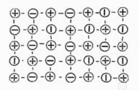
Figure 4 Molecular Structure Layout of Silicon
Silicon solar cells, also known as solar cells, are dominated by their excellent semiconductor performance. From the solar wings of artificial satellites to the solar panels for photovoltaic power generation, they all belong to the big family of silicon solar cells. Human beings have a long history of utilizing solar energy, but initially it was limited to the direct use of light and heat. The use of sunlight for power generation has been around since the 1950s. In 1839, corporate scientist Becquerel discovered that light can generate voltage in different parts of semiconductor materials, known as the "photovoltaic effect". Silicon solar cells designed based on photovoltaic effects are an effective way for people to utilize solar energy.
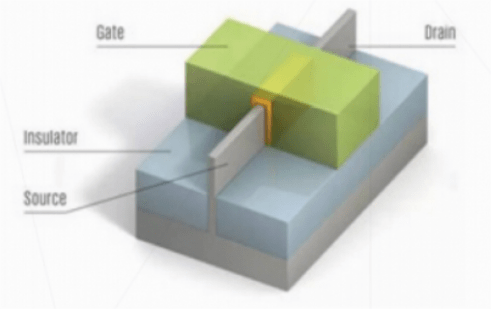
Figure 5 Process principle of silicon chips
When the IILA group element boron is doped, electrons are lacking in the silicon crystal, forming a P-type semiconductor. When the VA group element phosphorus is added, the silicon crystal will form due to the presence of residual electrons? N-type semiconductor. When P-type and N-type semiconductors are combined, a special thin film is formed. Due to electron diffusion, an internal electric field is formed from N to P, which prevents diffusion from occurring. After reaching equilibrium, such a special thin layer will form a potential difference, thus forming a PN junction as shown in Figure 6. When the chip is exposed to light, a current from the N region to the P region is formed in the PN junction due to electron flow. Then, a potential difference is formed in the PN junction, which forms the power supply. When the surface of a silicon solar cell is exposed to sunlight, there will be current flowing through the external circuit. Compared to amorphous silicon cells, monocrystalline silicon and polycrystalline silicon solar cells have advantages in conversion efficiency, lifespan, cost, and raw material supply, which have become the most ideal solar cells at present.
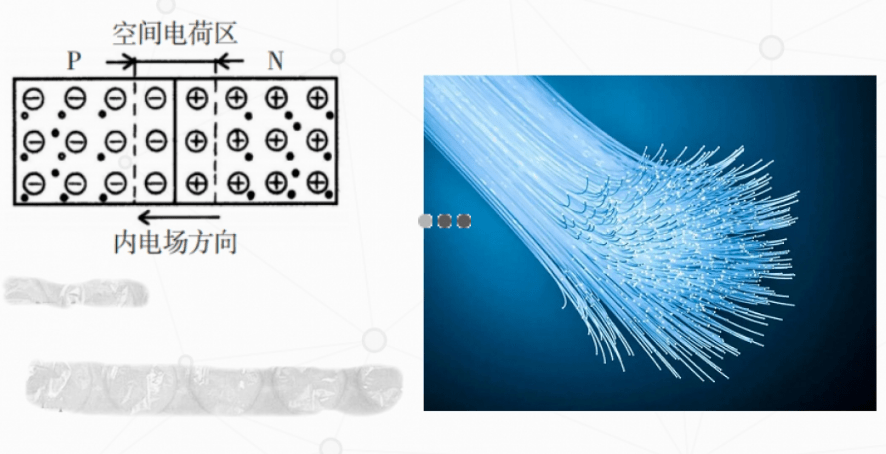
Figure 6 PN Structure
Figure 7 Silicon dioxide optical fiber
3.2 Silicon dioxide
Optical fiber, abbreviated as fiber optic, is a medium that relies on total reflection of light in a cable to transmit information using light as a carrier. Since light is used for transmission, it is required that the medium be as transparent as possible. Pure silica can produce high transparency glass fibers [Figure 7], and the cost is low. A glass fiber as thin as a hair can simultaneously transmit 256 calls, with high communication capacity, no electromagnetic interference, no fear of eavesdropping, and high confidentiality. Therefore, this fiber has become a leading figure in the field of optical fibers.
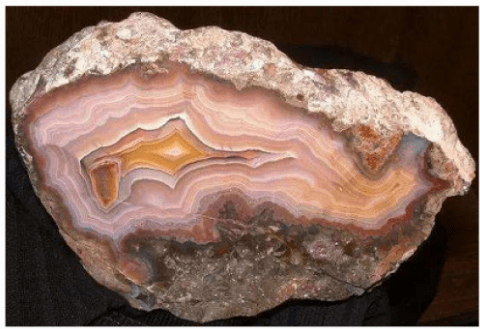
Figure 8 Agate
In addition, colorful agate [Figure 8], coastal gravel, beautiful crystals, hard flint [Figure 9], and so on, all of which are mainly composed of silica. In the eyes of different people, silica has different identities. In the eyes of geologists, silica is seen as quartz, flint, sand, etc. In the eyes of jewelry enthusiasts, it is also seen as decoration such as amethyst, opal, and agate. Among them, flint is dense and hard, and is one of the earliest minerals used by ancient humans when they began using tools. Our ancestors hammered it into scrapers, hammers, axes, etc. to obtain food and sustain their daily needs.
Figure 9 Flint
3.3 Silicates
Ceramics, glass, and cement are the three most commonly used inorganic non-metallic materials.
Cement is the basic material of modern architecture, and its main raw materials are lime, silicate, and aluminosilicate. The annual production of cement worldwide is about 4 billion tons, of which about half is produced by China. The most commonly used silicate cement at present was invented by the British man Asputin in 1824.
Glass is also a silicate product. Interestingly, there is natural glass in nature - obsidian. The chemical composition of obsidian is hydrated silica, with a predominantly black color and sharp shards. In the Stone Age, ancient humans extensively used obsidian, and in modern times, surgical blades made from obsidian are also used. Ordinary glass contains 75% silica. Adding various metals and metal oxides to glass can change its color and optical properties. Lenses made of glass have given birth to two scientific tools - telescopes and microscopes. With them, humans have greatly expanded their horizons and promoted the process of scientific development.
Porcelain is a silicate product first invented by the Chinese people. The formula composition of porcelain varies greatly, but the basic raw materials are still clay and kaolin (mainly composed of aluminosilicates). In the electrical industry, porcelain insulators are excellent high-voltage insulation materials; Ceramic tiles are beautiful, wear-resistant, impermeable, and easy to clean, making them the preferred choice for bathroom decoration; Dental porcelain is made of ceramics or composite materials, which can better mimic the appearance, structure, color, hardness of natural teeth, and have a palatability comparable to real teeth.
4. Conclusion
As a widely distributed element in nature, silicon is not only the darling of the computer age, but also the cornerstone of the Earth. It has long been integrated into every aspect of human life, not only hiding in the long river of history to witness the vicissitudes of the universe, but now, it has also appeared in various high-tech fields, becoming the "elite" of elements. Elements that are low-key to dust can also shine in the long river of history and the information age.
Technological innovation
Honesty is the foundation
Contact Number: +86-15698999555 |
Address: NO.6 ,SHENGHUA STREET,TAIHE DISTRICT, JINZHOU CITY, LIAONING PROVINCE, CHINA. |