1、 Introduction
Tantalum nitride thin film is an excellent piezoresistive material with a relatively complex structure, and there are currently as many as 11 known phases [1-3]. Tantalum nitride has advantages such as high stability, low resistance temperature coefficient, moderate strain factor, and excellent wear resistance. It is a widely used material in aerospace, microelectronics, power machinery, and other fields. In addition, compared to the commonly used nickel chromium alloy thin film materials, TaN thin film has better self passivation characteristics, can generate a dense Ta2O3 film in the air, and can work in an unsealed state to resist water vapor erosion, thus having excellent stability and reliability. Therefore, tantalum nitride thin film pressure sensors have broad application prospects, but tantalum nitride is a compound material that requires research on preparation and heat treatment processes to obtain stable and reliable pressure sensors.
2、 Working principle
The working principle of the thin film pressure sensor is shown in Figure 1. The thin film strain sensing principle is that the gas pressure P acts on the metal elastic body to cause deformation of the structure. DC ion beam sputtering and other technologies are used to make a thin film resistor on the elastic body structure to form an electric bridge. The deformation of the elastic body changes the resistance value of the strain resistor, and the electric bridge outputs an electric signal proportional to the pressure. By changing the thickness of the elastic structure, the pressure can be converted into displacement deformation to be transmitted to the thin film resistance, causing corresponding deformation of the resistance. Different range pressure sensors can be manufactured.

Figure 1 Strain Principle Diagram
3、 Structure and layout design
(1)Film thickness design
The design adopted a circular flat film structure as the pressure sensing element of the pressure sensor. When designing the steel cup structure, the problem of stress concentration at the edge of the membrane is solved by chamfering with R0.4 at the edge of the membrane, which can ensure that the membrane will not reach its elastic limit under overload of 200% of the full range condition.
At this point, the thickness design of the circular flat film is a key factor affecting the sensitivity of the sensor. The design thickness of the membrane is 0.5mm. After grinding and polishing to reduce the thickness by 40m, it was tested that there was no sudden change in the core performance under an overload of 130MPa.
(2)Strain map design
The radial and tangential strain formulas for the peripheral fixed flat film sheet are as follows [4]:

Among them: zh represents radial strain, zh represents tangential strain, zh represents uniformly distributed pressure (Pa), z represents Poisson's ratio of the membrane material, R is the radius of the flat membrane (cm), r is the radius of any part of the membrane (cm), E is the elastic modulus of the membrane material (Pa), and h is the thickness of the membrane (cm). The layout design is shown in Figure 2.
Figure 2 Strain Layout Design
As shown in Figure 2 (a), the radial strain and tangential strain at the center of the circle are tensile strains of equal magnitude, the radial strain at the edge of the flat membrane is compressive strain, and the tangential strain is zero. The layout design of thin film resistors should maximize the use of the strain region of the elastomer and improve output sensitivity. According to the principle of strain gauges, when the geometric symmetry of the shape of the strain resistance is completely consistent with the direction of stress distribution, the strain resistance value generated by the strain resistance is maximum. Therefore, during the design process, the maximum transformation of strain into resistance value variation is achieved, as shown in Figure 2 (b).
(3)Packaging design
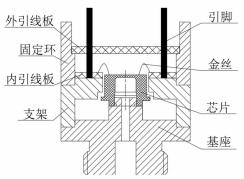
The sensor structure is shown in Figure 3. The sensor design range is 50MPa, the product diameter is less than 20mm, and the maximum failure pressure is 135MPa. Therefore, the main difficulties to consider in the sensor structure design are the 135MPa pressure resistance and the design of miniaturized packaging.

Figure 3 Packaging Structure Diagram
In the design of the sensor structure, an end face sealing structure is adopted, and the sensitive chip and base are sealed by laser welding. It has been verified through experiments that both the pressurized structure and the weld can withstand a pressure of 135MPa.
The traditional sputtering film chip packaging uses solder to fix the inner and outer lead plates, resulting in product diameters exceeding 28mm. To reduce the packaging size of the sensor, a lead bracket is selected to lead out the input and output of the chip. The lead is directly fixed to 5 0.8mm gold plated guide pins, and the base is fixed to the bracket through laser welding. The inner lead board passes through 5 gold-plated guide pins and is fixed on the bracket with solder. The chip is connected to the inner lead board by gold wire ball welding. The fixed ring and bracket are connected by laser welding, and the outer lead plate passes through 5 gold-plated guide pins and is soldered onto the card slot of the fixed ring, thereby achieving miniaturization and lightweight sensor packaging.
4、 Source experiment
The elastic material used for chips is 17-4PH stainless steel, with an elastic modulus greater than 197GPa. The flattening treatment of the stainless steel elastic substrate is completed through mechanical grinding and polishing. A buffer layer and insulation layer are deposited on a treated stainless steel elastic substrate using a direct current ion beam sputtering coating method. A direct current ion beam reactive sputtering deposition process was used to deposit tantalum nitride thin films on the insulation layer [5]. The target material was a 99.99% pure Ta target with a size of 110mm, 100mm, and 3mm. The sputtering gas used was a mixture of 99.99% argon and nitrogen gas, with a background vacuum of 9 I10-4Pa, a sputtering pressure of 2.7 I10-2Pa, a N2/Ar2 flow ratio of 3%, and a deposition time of 30 minutes.
The annealing process of the tantalum nitride thin film was completed using vacuum atmosphere heat treatment. The background vacuum was 5 μ g-10-2Pa, and argon gas was introduced as a protective gas. The annealing pressure was 0.1 Pa, the annealing temperature was 700 μ g, and the annealing time was 1 hour.
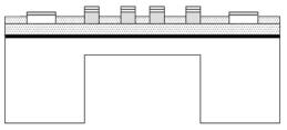
By ion beam etching of tantalum nitride thin films [6], four resistance bridges are formed to form a Wheatstone full bridge circuit. The internal resistance is distributed near the center of the elastic strain region, and the external resistance is distributed near the edge of the strain region. Using ion beam sputtering deposition technology, metal Ti (10nm), metal platinum (100nm), gold electrode (800nm), and passivation layer SiO2 (250nm) were sequentially deposited. The structure of each layer of thin film is shown in Figure 4.

Figure 4 Schematic diagram of thin film layer
5、 Results and Discussion
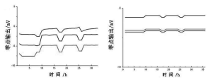
The influence of heat treatment process on zero point stability is shown in Figure 5. Figure 5 (a) shows the long-term stability data of the core zero point output without annealing process, and Figure 5 (b) shows the long-term stability data of the core zero point output after annealing treatment. From the graph, it can be seen that the zero drift of the sample without annealing process is very severe, and the maximum drift can reach 200 μ V under the same temperature environment, while the zero drift of the sensor after heat treatment at the same temperature is less than 5 μ V.

(a) No heat treatment (b) 700 Yi annealing for 1 hour
Figure 5 Effect of Heat Treatment Process on Zero Point Stability
Due to the multiple phases of TaN, the performance of the film may change under the influence of air or moisture before reaching a stable state, resulting in long-term drift of the film's resistance value [7]. After appropriate annealing treatment, the thin film reaches a stable chemical state, and its resistance significantly decreases due to changes in external conditions, which is reflected in a significant improvement in the zero point stability of the sensor.
The performance test results of the sensor are listed in Table 1. It can be seen from the table that the sputtered thin film pressure sensor using TaN as the sensitive material has excellent characteristics such as nonlinearity and high sensitivity.
Table 1 Sensor Performance Test Results
| Sample 1, Sample 2, Sample 3, Sample 4, Sample 5 |
Range (MPa) 50 50 50 50 50 Sensitivity (V/mV) 1.92 1.88 1.94 1.88 1.87 Nonlinear (% FS) 0.06 0.07 0.08 0.06 0.06 Repeatability (% FS) 0.03 0.02 0.02 0.02 0.03 Hysteresis (% FS) 0.02 0.02 0.02 0.02 0.02 Zero drift (% FS) 0.02 0.03 0.05 0.03 0.05 Thermal zero drift (% FS aid-1) 0.075 0.052 0.071 0.047 0.029 Thermal sensitivity drift (% FS Yi-1) 0.019 0.018 0.025 0.023 0.022 |
6、 Conclusion
A miniaturized and lightweight structure and strain pattern were designed for the study of the performance of tantalum nitride thin film pressure sensors. Functional tantalum nitride thin films were prepared by DC reactive ion sputtering method. The sensors were heat treated in a high-temperature annealing furnace at an annealing temperature of 700 ° C and an annealing time of 30 minutes. A tantalum nitride thin film pressure sensor chip with high zero stability was obtained.
The TaN sensitive material used in this sensor has excellent static performance characteristics, high sensitivity, and other characteristics. Compared to traditional nickel chromium sensitive materials, there are shortcomings such as more complex processes and poor temperature characteristics, which can meet the requirements of low temperature characteristics and high sensitivity for product applications.
Technological innovation
Honesty is the foundation
Contact Number: +86-15698999555 |
Address: NO.6 ,SHENGHUA STREET,TAIHE DISTRICT, JINZHOU CITY, LIAONING PROVINCE, CHINA. |