Ceramic matrix composites (CMCs) have excellent thermodynamic properties and low density, making them key structural materials for the new generation of high thrust to weight ratio aviation engine hot end components. In a high-temperature dry oxidation environment, a SiO2 protective film can be formed on the surface of ceramic matrix composites to resist the erosion of oxidizing substances. However, corrosive media such as high-temperature water vapor and molten salt exist in the service environment of aircraft engines, which can react with the SiO2 protective layer on the surface of CMCs, leading to rapid performance degradation [2]. Environmental barrier coatings (EBCs) can isolate ceramic matrix composites from corrosive media in the service environment, achieving the purpose of protecting the substrate material.
Rare earth silicate materials have good phase stability, excellent corrosion resistance, and thermal expansion coefficient matching with the substrate, making them the most promising environmental barrier coating materials [4]. However, rare earth silicate coatings are prone to defects such as pores and cracks during the preparation process, and the oxide secondary phase generated by decomposition can affect the service performance of the coating [5-8]. To improve the durability of EBCs, researchers from NASA have developed coating systems such as rare earth silicate/Si and rare earth silicate/mullite/Si [3]. Richards et al. [9] studied the failure mechanism of Yb2SiO5/mullite/Si coating under water oxygen corrosion conditions at 1316 ℃, and found that corrosive substances enter the interior with the penetrating cracks of the surface layer, causing the oxidation of the silicon bonding layer to form components β- Thermal growth oxide (TGO) of SiO2, β- SiO2 oriented α- The phase transition of SiO2 is accompanied by significant volume changes, resulting in a large number of microcracks and accelerating coating failure. The LaMgAl11O19/Yb2SiO5/Si coating designed by Li et al. [10] exhibited good corrosion resistance under water oxygen corrosion conditions at 1300 ℃. Guo et al. [11] proposed that the Hf0.84Y0.16O1.92/Yb2SiO5/Si coating has good stability in an air environment of 1300 ℃. The Yb2Si2O7/Si coating prepared by Wu et al. [12] using PS-PVD technology exhibits good service performance in water vapor environments between 1300 and 1450 ℃. Our research team replaced mullite with Yb2Si2O7 and designed a Yb2SiO5/Yb2Si2O7/Si coating, which has good thermal shock resistance and crack propagation resistance [13]. Although optimizing the design of coating structure can achieve the goal of protecting the substrate material from high-temperature water oxygen corrosion for a certain period of time, combined with failure analysis, it can be found that rare earth silicate EBCs still generate thermal stress during the thermal cycling process due to the mismatch of thermal expansion coefficient between the coating and the substrate, resulting in through cracks in the rare earth silicate surface layer.
To solve the problem of accelerated failure of EBCs system due to surface cracking during service, the use of silicide modified coating design to reduce crack propagation is another effective way to improve its durability. At present, research on the application of silicon containing compounds such as SiC and MoSi2 as self-healing agents in thermal barrier coatings has received attention, but there are few reports on using silicon containing compounds to modify rare earth silicate environmental barrier coatings [14]. Chen et al. [15] used TiSi2 doped Y2Si2O7 and prepared BSAS/TiSi2-Y2Si2O7/composite coatings using a slurry method. Research has found that TiSi2 oxidation products can fill through cracks in coatings, but BSAS has a lower long-term service temperature (<1300 ℃), which cannot meet the current development needs of EBCs [16]. Nguyen et al. [17] reduced 10% β- SiC (volume fraction, same below) was introduced into Yb2Si2O7 bulk materials containing Yb2SiO5 phase. After being heat treated in an air environment at 1250 ℃ for 2 hours, it was found that SiC oxidized to form SiO2, which can fill cracks. Kunz et al. [18] studied the crack self-healing behavior of ytterbium silicate at higher temperatures (1400 ℃) and longer durations (200 hours), and found that Yb2Si2O7 bulk material doped with 1% SiC had the best crack self-healing and performance. Vu et al. [19] found that the crack self-healing effect of 5% SiC/Y2SiO5 bulk material is better than that of 5% SiC/Y2Si2O7, and Y3+diffusion has positive significance for crack self-healing.
MoSi2 is the intermetallic compound with the highest Si content in the Mo Si system, characterized by high melting point and good thermal oxidation stability [20-21]. It has excellent oxidation resistance at high temperatures [22] and has been widely used in high-temperature oxidation resistant coatings. Introducing MoSi2 into rare earth silicate (Yb2SiO5) coatings is expected to improve the high-temperature stability of rare earth silicate EBCs systems. However, the effect of MoSi2 doping on the thermal shock resistance of rare earth silicate EBCs systems has not been accurately studied. This work adopts vacuum plasma spraying technology to prepare a new Yb2SiO5-MoSi2/Yb2Si2O7/Si coating system with MoSi2 modified Yb2SiO5 (MoSi2 doping amount of 5%, 10%) as the surface layer on SiC substrate. The resistance to water quenching thermal shock behavior at 1350 ℃ is studied, and the modification mechanism of MoSi2's resistance to thermal shock and crack propagation is explored based on the microstructure characterization results of the coating.
1. Experimental Materials and Methods
1.1 Experimental Materials
Yb2SiO5 and Yb2Si2O7 powders were prepared using solid phase reaction method using Yb2O3 powder (Shanghai Heli Rare Earth Group Co., Ltd.) and SiO2 powder (China National Pharmaceutical Group Chemical Reagent Co., Ltd.) as raw materials. Mix Yb2SiO5 and MoSi2 powders in a volume ratio of 95:5 and 90:10 to obtain powders suitable for spraying.
Experiment selection 25.4 mm × 3mm SiC ceramic plate as the substrate. To obtain a clean and rough surface, it is necessary to sandblast the substrate before spraying. Si and Yb2Si2O7 powders were sequentially sprayed onto the substrate using vacuum plasma spraying technology (VPS, A-2000), followed by Yb2SiO5, Yb2SiO5-5% MoSi2, and Yb2SiO5-5% MoSi2, respectively. For the convenience of explanation, coatings with 5% MoSi2 and 10% MoSi2 additions are designated as Y5M and Y10M, respectively, while Yb2SiO5 and Yb2Si2O7 are designated as YbMS and YbDS, respectively. Finally, YbMS/YbDS/Si, Y5M/YbDS/Si, and Y10M/YbDS/Si coatings were obtained.
1.2 Experimental Methods
The water quenching thermal shock experiment was conducted in the QGF1600-60 tubular furnace. Place the coating sample in a tube furnace at 1350 ℃ for 10 minutes, then quickly remove the sample and quench it in deionized water at room temperature, and then dry the sample. The above is one water quenching thermal shock cycle, and the experiment ends after a total of 40 cycles or after the coating peels off.
Observe the macroscopic morphology of the sample before and after thermal shock experiment using an optical microscope (OM, E3CMOS). Field emission scanning electron microscopy (SEM) was used to analyze the surface and cross-sectional microstructure of the coating. Before testing the sample of the analysis section, metallographic polishing treatment is required, followed by cleaning and drying with anhydrous ethanol.
2 Results and Analysis
2.1 Microstructure and thermal shock resistance behavior of different coatings
Figures 1 (a) to (c) show the SEM cross-sectional morphology of three sprayed EBCs coatings: YbMS/YbDS/Si, Y5M/YbDS/Si, and Y10M/YbDS/Si. It can be seen that the three coating systems all contain a three-layer structure of rare earth monosilicate surface layer, pyrosilicate intermediate layer, and silicon bonding layer. Each layer of coating has a small amount of defects such as pores and microcracks. The interface bonding between each layer of the coating is good, and there are almost no defects such as pores and cracks at the interface. Figure 1 (d) shows the high magnification morphology of the Y5M surface layer doped with MoSi2 region. Based on EDS analysis results, it can be seen that the gray contrast region (point 2) is Yb2SiO5, and the black contrast region is MoSi2 (point 1). The composition of the Mo containing region is uniform and well combined with the Yb2SiO5 region.
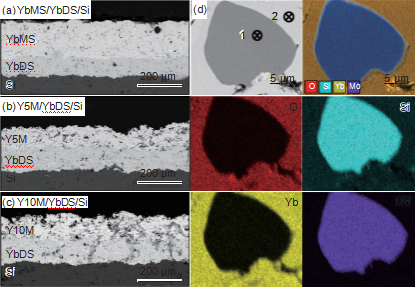
Figure 1 SEM cross-sectional morphology of sprayed EBCs coating (a) YbMS/YbDS/Si; (b) Y5M/YbDS/Si;
(c) Y10M/YbDS/Si; (d) High magnification morphology and EDS element distribution map of Y5M surface layer

Figure 2 Macro morphology of different EBC coatings before and after thermal shock
Figure 2 shows the macroscopic morphology before and after water quenching and thermal shock at 1350 ℃. It can be seen that after 20 thermal shocks, the SiC substrate exhibits fragmentation. The Y5M/YbDS/Si and Y10M/YbDS/Si coating systems have good integrity, but the YbMS/YbDS/Si coating system exhibits slight peeling at the edge of fragmentation. After 40 thermal shocks, the Y5M/YbDS/Si and Y10M/YbDS/Si coatings remained intact, but the peeling area of the YbMS/YbDS/Si coating did not significantly increase, indicating that the peeling of the coating may be caused by matrix cracking.

Figure 3 SEM surface morphology of three coating systems after 40 thermal shocks
(a) YbMS/YbDS/Si; (b) Y5M/YbDS/Si; (c) Y10M/YbDS/Si
Figure 3 shows the surface morphology of three coating systems after 40 water quenched thermal shocks at 1350 ℃. It can be seen that there are cracks on the surface of all three coating systems, and the YbMS/YbDS/Si coating without MoSi2 doping has more surface cracks.
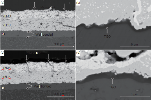
Figure 4 SEM cross-sectional morphology of YbMS/YbDS/Si coating (a)~(b) with 20 thermal shocks; (c) ~(d) 40 thermal shocks
Figure 4 shows the cross-sectional morphology of the YbMS/YbDS/Si coating system after 20 and 40 water quenched thermal shocks at 1350 ℃. From Figure 4, it can be seen that the bonding between the layers of the coating and the substrate is good, and there is no cracking phenomenon between the layers. The Yb2SiO5 surface layer is generated by longitudinal cracks, but the cracks do not penetrate the entire coating and terminate in the middle layer of Yb2Si2O7. A SiO2 TGO layer with a thickness of about 400 nm can be observed at the YbDS/Si interface after 20 thermal shocks, and there are no cracks inside the TGO layer. After 40 thermal shocks, the number of longitudinal cracks in the Yb2SiO5 surface layer increased, and the thickness of the TGO layer at the YbDS/Si interface was about 900nm.
The SEM cross-sectional morphology of the Y5M/YbDS/Si coating system after 20 and 40 water quenching shocks at 1350 ℃ is shown in Figure 5. It can be seen that the bonding between the coating and the substrate, as well as between each layer of the coating, is good. After 20 thermal shocks, penetrating cracks were generated in the Y5M surface layer and terminated at the Y5M/YbDS interface (Figure 5 (a)). A TGO layer with a thickness of about 150 nm was observed at the YbDS/Si interface, but no obvious cracks were observed within the TGO layer. The structure was intact and well combined with Yb2Si2O7 and Si (Figure 5 (b)). After 40 thermal shocks, the longitudinal cracks in the Y5M layer still terminated at the Y5M/YbDS interface and deflected (Figure 5 (c)), while the thickness of the TGO layer did not significantly increase (the TGO layer thickness was still 150 nm) (Figure 5 (d)).
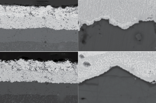
Figure 5 SEM cross-sectional morphology of Y5M/YbDS/Si coating (a)~(b) with 20 thermal shocks; (c) ~(d) 40 thermal shocks
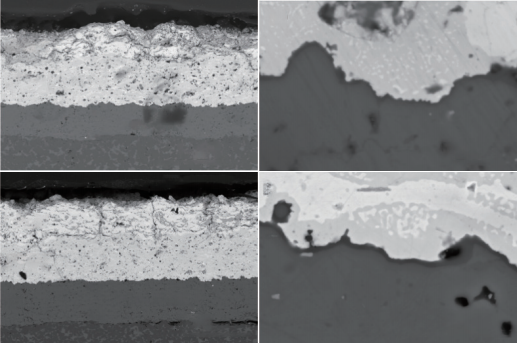
Figure 6 SEM cross-sectional morphology of Y10M/YbDS/Si coating (a)~(b) with 20 thermal shocks; (c) ~(d) 40 thermal shocks
Figure 6 shows the SEM cross-sectional morphology of Y10M/YbDS/Si coating after 20 and 40 water quenched thermal shocks at 1350 ℃. It can be seen that after 20 thermal shocks, there are almost no longitudinal cracks generated in the Y10M surface layer (Figure 6 (a)), and a TGO layer with a thickness of about 100 nm can be observed at the YbDS/Si interface (Figure 6 (b)). After 40 thermal shocks, longitudinal cracks appeared in the Y10M surface layer and terminated in the Yb2Si2O7 layer (Figure 6 (c)). The thickness of the TGO layer was about 100nm, and it bonded well with Yb2Si2O7 and Si (Figure 6 (d)).
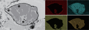

Figure 7 SEM cross-sectional morphology of Y5M and Y10M surface layers after different thermal shock times (a) Y5M surface layer thermal shock 20 times and EDS element distribution diagram; (b) 20 thermal shocks on the Y10M surface layer; (c) Y5M surface thermal shock 40 times; (d) 40 thermal shocks on Y10M surface layer
Figure 7 shows the SEM cross-sectional morphology and related EDS analysis results of the doped MoSi2 coating system before and after thermal shock at 1350 ℃. It can be seen that after 20 thermal shocks, MoSi2 undergoes transformation and exhibits various contrasts. Based on the analysis of Figure 7 (a) and EDS (Table 1), it can be seen that the black contrast component around the surface Mo rich area is SiO2 (point 3), and there are unoxidized MoSi2 (point 6) and oxidized Mo5Si3 (points 4 and 5) inside the Mo rich area. This indicates that MoSi2 undergoes slight oxidation during the thermal shock process. The MoSi2 and Mo5Si3 in the rich Mo region combine well (Figure 7 (b)). The microcracks generated by thermal stress in the Y5M and Y10M surface layers deflect near the Mo rich region (Figure 7 (c) and (d)). This phenomenon can prolong the propagation path of cracks inside the Y5M and Y10M coatings, consuming more fracture energy during propagation, making it difficult for cracks to penetrate the entire surface layer. However, the presence of SiO2 was not observed inside the cracks, which may be related to shorter oxidation time and lower SiO2 content.
EDS element composition (atomic fraction/%) of labeled areas in Figures 1 and 7 of Table 1
Spectrum location Yb Si O Mo
Point 1 ---- 61.02 5.05 33.93
Point 2 39.07 12.42 48.51 -----
Point 3 5.0153.68 36.28 5.03
Point 4 ----- 44.77 ----- 55.23
Point 5 ----- 41.83 ----- 58.17
Point 6 ----- 70.32 ----- 29.68
Point 7 20.8324.08 55.08 -----
Figure 7 SEM cross-sectional morphology of Y5M and Y10M surface layers after different thermal shock times (a) Y5M surface layer thermal shock 20 times and EDS element distribution diagram; (b) 20 thermal shocks on the Y10M surface layer; (c) Y5M surface thermal shock 40 times; (d) 40 thermal shocks on Y10M surface layer
Figure 7 shows the SEM cross-sectional morphology and related EDS analysis results of the doped MoSi2 coating system before and after thermal shock at 1350 ℃. It can be seen that after 20 thermal shocks, MoSi2 undergoes transformation and exhibits various contrasts. Based on the analysis of Figure 7 (a) and EDS (Table 1), it can be seen that the black contrast component around the surface Mo rich area is SiO2 (point 3), and there are unoxidized MoSi2 (point 6) and oxidized Mo5Si3 (points 4 and 5) inside the Mo rich area. This indicates that MoSi2 undergoes slight oxidation during the thermal shock process. The MoSi2 and Mo5Si3 in the rich Mo region combine well (Figure 7 (b)). The microcracks generated by thermal stress in the Y5M and Y10M surface layers deflect near the Mo rich region (Figure 7 (c) and (d)). This phenomenon can prolong the propagation path of cracks inside the Y5M and Y10M coatings, consuming more fracture energy during propagation, making it difficult for cracks to penetrate the entire surface layer. However, the presence of SiO2 was not observed inside the cracks, which may be related to shorter oxidation time and lower SiO2 content.
2.2 Exploration of MoSi2 Modification Mechanism
The above research indicates that both YbMS/YbDS/Si and YxM/YbDS/Si coating systems have good thermal shock resistance. After 40 thermal shocks, the coating system remained intact, and the surface layer developed through cracks, but terminated in the middle layer of Yb2Si2O7. This is closely related to the lower thermal expansion coefficient, smaller elastic modulus, and good plastic deformation ability of Yb2Si2O7 coating [23-24]. Figure 8 shows the comparison of TGO layer thickness for three coatings after different thermal shock cycles. It can be seen that compared to the TGO thickness in the YbMS/YbDS/Si coating system, the TGO thickness in the YxM/YbDS/Si coating system is smaller, indicating that the coating system modified with MoSi2 can effectively slow down the penetration of oxidizing substances. During the thermal shock process, MoSi2 in the doped modified surface layer undergoes oxidation and transforms into a mixed phase of MoSi2 and Mo5Si3. At the same time, SiO2 phase can be observed at the edge of the Mo rich zone, and Yb2Si2O7 phase also appears in the surface layer.
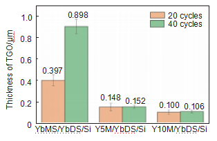
Figure 8 Comparison of TGO Layer Thickness of Three EBCs Coatings after Different Thermal Shock Times
Based on the above results, it can be inferred that MoSi2 undergoes the following reactions during the thermal shock process [25]:
5MoSi2 (s)+7O2 (g)! Mo5Si3 (s)+7SiO2 (s) (1)
SiO2 (s)+Yb2SiO5 (s)! Yb2Si2O7 (s) (2)
In a high-temperature oxidation environment, MoSi2 in the surface layer undergoes the above oxidation reaction, slowing down the erosion of the bonding layer by oxidizing substances. As the doping amount of MoSi2 increases, the oxidation resistance of the coating system improves.
The microcracks deflect near the Mo rich region, changing the longitudinal crack propagation path, preventing the cracks from directly penetrating the YxM coating, which is related to the good damage tolerance of MoSi2. The damage tolerance of ceramic materials can be compared through quantitative calculations. The brittleness index (B) [26] and damage tolerance parameter (Dt) [27] are commonly used quantitative indicators, with lower B and higher Dt indicating that the material has good damage tolerance. The calculation method is as follows:
B=Hv/KIC (3)
Dt=KIC · E/( σ · Hv) (4)
In the formula, Hv is the Vickers hardness of the material; KIC is the fracture toughness of the material; E is the Young's modulus of the material; σ The bending strength of the material.
The Hv of MoSi2 bulk material is 10.6 GPa, and the KIC is 4.5 MPa? M1/2, σ 560 MPa, E is 430GPa. It can be calculated that the B value of MoSi2 is 2.36 μ M1/2, lower than Yb2Si2O7 (2.78 μ M1/2) and Yb2SiO5 (3.40 μ M1/2), with a Dt value of 0.33 m1/2, between Yb2Si2O7 (0.38 m1/2) and Yb2SiO5 (0.25 m1/2) [28]. Therefore, this material has better damage tolerance than Yb2SiO5 material, which can prevent the diffusion of micro cracks into its interior. During the oxidation process, SiO2 often reacts directly with Yb2SiO5 through reaction 2. It can be inferred that as time increases at high temperatures, more Yb2Si2O7 will appear at the edge of the Mo rich zone. Thermal expansion coefficient of Yb2SiO5 coating (6.9~7.6) × 10-6K-1) is higher than Yb2Si2O7 coating (3.3-5.2) × 10-6K-1). Compared with Yb2SiO5 coating, Yb2Si2O7 coating has a lower elastic modulus. The coating has a high coefficient of thermal expansion and elastic modulus, and is subjected to significant thermal stress during thermal shock [29]. Therefore, the formation of Yb2Si2O7 is beneficial for reducing thermal stress during thermal shock. Based on the above analysis, MoSi2 has the following modification effects in the surface layer: (1) MoSi2 has good damage tolerance, which can effectively prevent the diffusion of cracks into its interior; (2) MoSi2 can consume oxidants and reduce the concentration of oxidants inside the coating.
3 Conclusion
(1) The YbMS/YbDS/Si, Y5M/YbDS/Si, and Y10M/YbDS/Si coating systems have dense structures and good bonding between each layer. When the doping amount of MoSi2 is 5% and 10%, the coating system has good thermal shock resistance.
(2) Doping MoSi2 can improve the damage tolerance of YxM coatings, and the Yb2Si2O7 formed by oxidation reaction has lower thermal expansion coefficient and elastic modulus, which is beneficial for improving its thermal shock resistance.
(3) The TGO layer thickness in the YxM/YbDS/Si coating system is reduced by about 83% and 88% compared to the YbMS/YbDS/Si coating system, respectively. The Y10M/YbDS/Si coating system with more MoSi2 doping has the smallest TGO layer thickness. The oxidation of MoSi2 can consume oxidizing media and reduce its diffusion into the coating system, which is beneficial for slowing down the oxidation of the bonding layer.
Technological innovation
Honesty is the foundation
Contact Number: +86-15698999555 |
Address: NO.6 ,SHENGHUA STREET,TAIHE DISTRICT, JINZHOU CITY, LIAONING PROVINCE, CHINA. |