LaB6 material has excellent electron emission performance and stable chemical properties, and is widely used in various high current and long-life electron emission devices, such as high-energy accelerators, dynamic high-power traveling wave tubes, electron beam injection machines, ion sources, and high current pulse electron sources. In large-area, high current, and long-life cathode applications, the use of LaB6 blocks is limited to some extent. For example, the growth conditions of LaB6 single crystals are harsh, and the growth process is complex, making it very difficult to prepare large-area single crystal LaB6 cathodes; The preparation of LaB6 polycrystalline materials requires a high-temperature and high-pressure environment, and the cost of preparing large-sized polycrystalline LaB6 cathodes is high. Compared to LaB6 single and polycrystalline bulk materials, the preparation conditions for LaB6 thin films are lower, the preparation process is simple, and it is easy to prepare LaB6 thin film cathodes with large or complex surface morphology, resulting in lower preparation costs. Therefore, it is very important to study the preparation method and performance of LaB6 thin films on large area substrates. At present, there are three main methods for preparing LaB6 thin films: electron beam evaporation, magnetron sputtering, and chemical vapor deposition. The thin film prepared by magnetron sputtering method has residual atoms of protective gas and character defects, resulting in high internal stress and easy detachment after film formation. The deposition rate of LaB6 thin films prepared by chemical vapor deposition method is slow, only 1-2% μ M/h, when preparing, the substrate temperature is required to be very high, and the escape work of the prepared sample is 2.70eV, which is the highest among the three methods of sample preparation. The LaB6 thin film prepared by electron beam evaporation method has uniform film formation, and the preparation process does not require heating the substrate. There are no special requirements for the substrate material, making it easy to prepare large area and well uniform LaB6 thin films. In this paper, LaB6 thin films were prepared on glass and tantalum/tantalum carbide (Ta/TaC) substrates using electron beam evaporation. The surface structure and morphology of LaB6 thin films were studied using X-ray diffraction (XRD) and scanning electron microscopy (SEM) at different evaporation angles; The thermal electron emission method was used to study the escape work of LaB6 thin films.
1 Experiment
Experiment selection 80mm × A 40mm glass substrate was deposited with LaB6 thin film using point source electron beam evaporation method, with a distance of 20mm between the LaB6 target and the substrate glass. The deposition parameter is: vacuum degree 2 × 10 * Pa, substrate temperature 250 ℃, LaB6 target temperature 2300 ℃, evaporation time 20 minutes.
In order to study the work function of LaB6 thin film, LaB6 thin film was prepared on a Ta substrate covered with a TaC protective layer. The function of TaC was to prevent the reaction between LaB6 thin film and Ta substrate during the high-temperature process. LaB6 thin film was deposited under the same process conditions as on a glass substrate, with a deposition time of 5 minutes. The deposited samples were subjected to thermal electron emission testing, and the escape work was calculated according to Richardson's formula. The surface morphology of LaB6 thin films was studied using SEM.
2 Crystal planes and adhesion properties of 2 LaB6 thin films
In order to study the relationship between the LaB6 thin film of electron beam Yan Fa and the properties of raw materials, crystal plane analysis was first conducted on the LaB6 polycrystalline target material. Figure 1 shows the XRD diffraction pattern of LaB6 target material for evaporation, and Figure 2 shows the LaB6 thin film evaporation device. The diffraction peaks of the target XRD pattern correspond to crystal planes (100), (110), (111), (200), (210), and (211). Numerous studies have shown that the electron emission performance of LaB6 is related to the crystal plane, with the (100) crystal plane having the best overall electron emission performance. This article mainly studies the relationship between the (100) crystal plane and preparation process of LaB6 thin films.
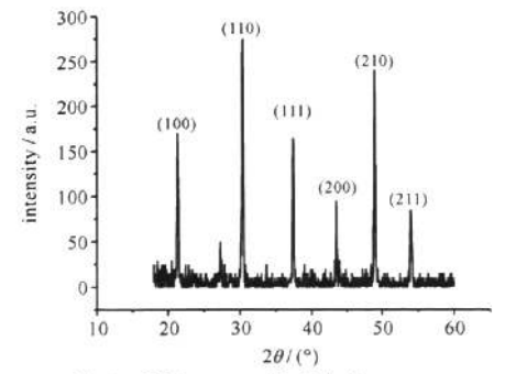
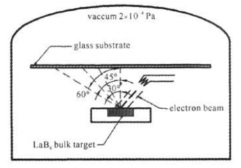
Figure 1 XRD Pattern of LaB6 Block Figure 2 Electron beam evaporation 1aB6 thin scale experimental setup
XRD testing was performed on the prepared LaB6 thin film samples based on different evaporation angles. To eliminate the impact of noise on the test data during the testing process, exponential function convergence iterative fitting is used to obtain a smooth baseline for the base noise data; Then, the Gaussian function is used to converge and iterate to fit the diffraction peak; Finally, retain the original XRD test pattern to obtain Figure 3. From the test results, it can be seen that the X-ray diffraction peak distribution of the LaB6 thin film sample is basically consistent with that of the polycrystalline LaB6 target material, and there is no complete elimination of any peak. Therefore, the LaB6 thin film prepared by electron beam evaporation method will not completely eliminate the influence of target orientation within the evaporation angle of 60 °. Due to the fact that the crystal plane of LaB6 material is mainly determined by the framework composed of B atoms, the thermal evaporation rate of B atoms varies among different crystal planes of the target material, making it difficult for the thin film to grow along a single orientation.
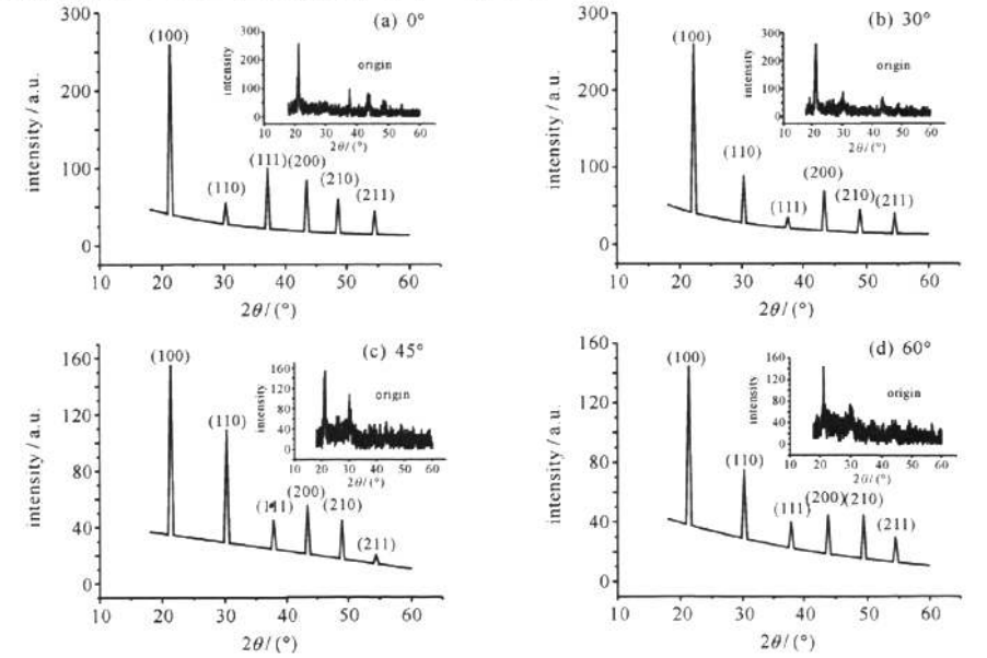
Figure 3 XRD patterns of LaB thin films prepared at different evaporation angles
By analyzing the XRD pattern, the diffraction multiplicity factor is set to P, and the structure factor of the product is FHKL (where H, K, L are the crystal plane indices). According to the polycrystalline relative emissivity formula 1cPFi2HKL, it can be seen that LaB6 thin films prepared at different evaporation angles all exhibit (100) crystal plane preferential growth. According to the theory of thin film growth, atoms or atomic groups need a certain substrate temperature for migration when nucleating at the substrate interface. In the preparation process, the designed substrate temperature is 250 ℃, and the nucleation and migration speed of the thin film is relatively low, which is not conducive to the growth of large index surfaces. The arrangement potential energy of B atoms on the (100) crystal plane is the lowest, thus obtaining preferential oriented growth.
By using the Scherrer formula, the grain size of the (100) crystal plane at different evaporation angles can be calculated
D= k λ (1)
Β Cos (2 θ)
In the formula, k=0.89 is the Scherrer constant; Characteristic wavelength of X-rays λ= 0.154nm; The radian value corresponding to the half width of the main peak of the sample is β; two θ Is the Bragg angle of the diffraction peak; D is the grain size. According to the fitting processing curve, the half width at half height (FWHM) was obtained, and the grain size calculated from the half width at half height is shown in Table 1.
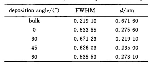
Table 1 Grain Linearity of Yanfa at Different Evaporation Angles
Analyzing the grain size of the (100) product surface, it can be concluded that at 0 ° evaporation, due to the highest density of atomic planes incident on the substrate, it is easy for grain growth, resulting in the highest grain size. When the evaporation angle is between 30 ° and 45 °, the atomic surface density incident on the substrate is lower than the surface density evaporated at 0 °, resulting in a smaller grain size. When the evaporation angle is 60 °, due to the shadow effect of thin film growth, the grain size increases. Overall, it can be concluded that when the evaporation angle is between 30 ° and 45 °, the grain size grown is smaller and it is easy to form small stress adhesion with the substrate.
The lattice constant of the (100) crystal plane at different evaporation angles can be determined by the lattice formula
 (2)
(2)
In the formula: characteristic wavelength of the ray λ= 0.154 nm; two θ Is the Bragg angle of the diffraction peak; A is the lattice parameter. Calculate the lattice parameters as shown in Table 2.
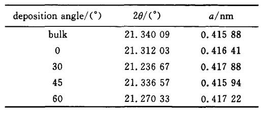
Table 2 Lattice Constants of Evaporated Thin Films at Different Evaporation Angles
Analyzing the (100) crystal plane, it was found that the lattice constant of the (100) crystal plane of the 45 ° evaporated film has the smallest difference from the lattice constant of the target material. The lattice deformation of the (100) crystal plane in the film is the smallest, and the internal stress in the film is the smallest. Based on grain size analysis, it is found that when the evaporation angle is 45 °, the LaB6 thin film prepared has fine and dense grains and low internal stress.
3 LaB6 thin film escape work
LaB6 thin film cathode was prepared at 45 ° on a Ta substrate with a sintered TaC protective layer, and the prepared LaB6 thin film cathode samples were subjected to hot electron emission testing. The electron emission formula under an accelerating field is  (3)
(3)
Derived from the deformation of Richardson's formula
 (4)
(4)
In the formula: a is a constant determined by the structural shape of the electrode system and the distance between electrodes; Ua is the applied anode voltage; Io is zero field emission current; A is the cathode emission constant; S is the cathode emission area; Φ Is the cathode work function; K is the Boltzmann constant; T is the cathode temperature. The escape work of LaB6 thin film can be calculated from equations (3) and (4).
Due to the high external anode voltage Ua, the influence of space charge and contact potential difference can be ignored. Under certain temperature conditions, draw the relationship curve between IgIa and Ua1/2, as shown in Figure 4. According to the different temperatures, fit the scattered points in Figure 4 into 5 straight lines, and then extend the lines to intersect with the ordinate. The intersection point is the zero field emission current Igl0 of the LaB6 thin film cathode at different temperatures. After substituting the zero field emission current and test parameters into equation (4), the correlation line between 1/T and lg (I0/T2) can be fitted, as shown in Figure 5. Based on the slope of the line in Figure 5 and equation (4), the escape work of the thin film sample can be calculated φ。
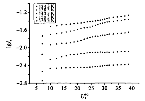
Figure 4 LaB, Voltammetric Characteristics of Thin Films at Different Temperatures
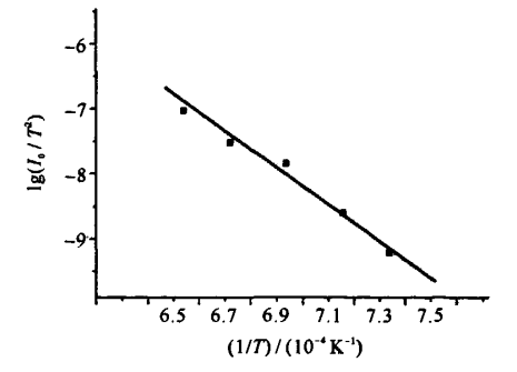
Figure 5 Richardeon Line Diagram of LaB Thin Film
According to equation (4) and Figure 5, the calculated work of LaB6 thin film cathode sample is 2.56eV. It is consistent with the low escape work property of LaB6 material (100) crystal plane, which also proves that LaB6 thin film is grown preferentially on the (100) crystal plane.
The SEM pattern of LaB6 thin film deposited on Ta/TaC substrate at an evaporation angle of 45 ° is shown in Figure 6. Compared to the porous structure of LaB6 target material, the LaB6 thin film prepared has good uniformity, no obvious step defects on the surface, and the film formation is very dense.
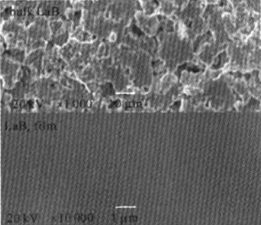
Figure 6 SEM patterns of Lalk, flower material, LaB, and thin film on TaC
4 Conclusion
This article uses electron beam evaporation to deposit LaB6 thin films on a large area glass substrate, achieving uniform and dense deposition of LaB6 thin films on a large area substrate. Through the analysis of the phase, particle size, lattice constant, and escape work of the thin film, it is concluded that LaB6 thin film grows preferentially on the (100) crystal plane at a substrate temperature of 250 ℃; When the evaporation angle is 45 °, the grains of the film are fine and dense, and the internal stress is small; The LaB6 thin film cathode prepared at a 45 ° angle on Ta/TaC has an escape work of 2.56 eV, and the film formation is uniform and dense.
Technological innovation
Honesty is the foundation
Contact Number: +86-15698999555 |
Address: NO.6 ,SHENGHUA STREET,TAIHE DISTRICT, JINZHOU CITY, LIAONING PROVINCE, CHINA. |